- Company
- Products
- Technical report
- Indusrial cleaning
- Micro Joining and Assembly Technology
- Ultrasonic technology
- Trouble solution
- Cleaning
- Removing
- Attaching
- PCB Columns
Published on :
A printed circuit board is a type of electronic component with wiring inside or on the surface of a board-shaped insulator.
KAKEN TECH develops and manufactures flux cleaning systems that clean flux residue after electronic components are soldered to electrodes on printed circuit boards.
This page describes the "printed circuit board" to which electronic components are soldered, which is closely related to flux cleaning.
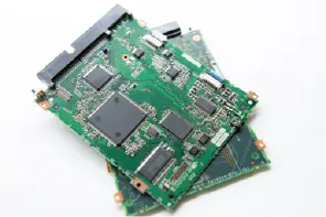 |
Although printed circuit boards are not often seen, the green plate-like objects found inside electronic devices and appliances around us are examples of printed circuit boards (left figure). Printed circuit boards is a generic term for ・Printed wiring board (board with circuit wiring) ・Electronic circuit board (electronic components such as capacitors and transistors soldered on a printed wiring board). |
| In this page, printed wiring boards are called printed circuit boards, and their types, structures, and manufacturing processes are explained. |
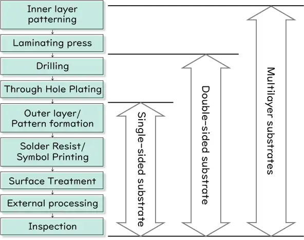
Printed circuit boards are classified according to the number of layers containing conductor circuits as follows,
| Cross-section view | Product examples | Explanation |
|---|---|---|
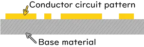 Single-sided substrate | Consumer electronic equipment (TVs, etc.) Mass-produced consumer electronics for cost reduction | Substrate with a structure in which a conductor circuit is formed on only one side. |
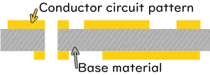 Double-sided substrate | Consumer electronics, industrial equipment, high-reliability equipment, and many other fields | A substrate with a structure in which conductor circuits are formed on both sides of the base material. It enables higher-density wiring than single-sided printed circuit boards, and has developed in line with the higher integration of components and the increased functionality of products. |
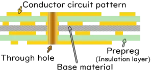 Multilayer substrates | Industrial electronic equipment, consumer mobile electronic equipment, and other fields requiring light, thin, small, and high-density mounting | Substrate with a structure of three or more layers of circuitry consisting of the conductor circuit inside the substrate and on the surface layer. |
A wide variety of base materials for printed circuit boards are used according to the application and needs of printed circuit boards, such as heat resistance, high-frequency characteristics, and high reliability.
Commonly used substrates include the following,
Printed circuit board made of paper impregnated with phenolic resin.
Due to its high water absorption and low insulation resistance, it is not suitable for products requiring long-term reliability or high-density mounting.
Because of its low cost, it is used in general household appliances, toys, electronic crafts, and self-made circuit boards.
A printed circuit board made of glass fiber impregnated with epoxy resin, sometimes referred to as glass epoxy or FR-4.
Because of its excellent insulation resistance and heat resistance and low coefficient of thermal expansion, it is widely used as a multilayer substrate that requires reliability and high-density mounting.
Printed circuit board based on 96% pure alumina, with excellent heat dissipation and insulation properties, and a low coefficient of thermal expansion.
They are used as printed circuit boards and highly reliable boards on which high heat-generating components must be mounted to dissipate heat.
However, it is not widely used due to its high manufacturing cost and shock resistance, and is used as a printed circuit board for some specific module products.
A printed circuit board with an insulating layer on a base material such as aluminum, iron, or copper, on which a circuit is formed.
Because of its excellent thermal conductivity and ability to suppress temperature rise due to component heat generation, it is used in power supply boards, power modules, etc., where heat dissipation is required.
Flexible printed circuit boards are made of polyimide resin or polyester resin and are sometimes referred to as FPCs or flexible substrates.
Since the base material is light and thin, it is used in devices and modules that require lightness and weight reduction. Also, since the base material is flexible, it is used as a printed circuit board for forming wiring to movable or curved parts.
| Printed circuit boards are generally manufactured by the following processes. |
 |
| Each process is introduced using a multilayer printed circuit board as an example. |
| Inner layer patterning |  |
Circuit patterns are formed by etching on copper clad wiring boards for the inner layer. |
|---|---|---|
| Laminating press |  | The surface of the copper circuit is roughened to improve adhesion to the prepreg, which serves as the insulation layer, and the prepreg and inner layer materials are alternately combined and heat-pressed to form the product. |
| Drilling |  | Drill holes in the printed circuit board using a drill machine. |
| Through Hole Plating | 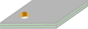 | Plating is applied in the through-holes to make each layer conductive. |
| Outer layer/pattern formation | 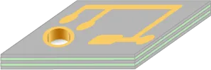 | Forms circuit patterns on the surface. |
| Solder Resist/Symbol Printing |  | Once the entire circuit is completed, solder resist is applied to protect the circuit surface. |
| Surface Treatment | 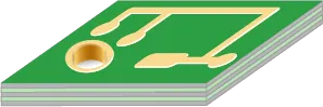 | Solder coat treatment and pre-flux treatment are performed to prevent copper surfaces of electrode pads from contamination, oxidation, and rusting. |
| External processing | 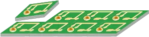 | Cut the sheet substrate to piece size. |
| Inspection |  | Inspect performance and appearance. |
 |
Fifth-generation mobile communications (5G communications) are expected to become the mainstream in the future. While the frequency band below 2.5 GHz has been used for communications up to now, the use of the high-frequency band above 6 GHz has been put to practical use in 5G communications. For example, in-vehicle radar systems that avoid collisions between automobiles are increasingly using radar in the 60-70 GHz band. |
| Future devices must be able to handle high-frequency signals. The high-frequency countermeasure for printed circuit boards is "low dielectric properties."In addition to selecting insulating materials with low dielectric loss, it is effective to perform flux cleaning (cleaning flux residue, which is a dielectric) after soldering. |
Standard Micro Soldering Technology, 3rd Edition
Japan Welding Engineering Society, Micro Soldering Education Committee [ed.]
Nikkan Kogyo Shimbun
 |
Trouble solution
|
|---|---|
 |
Technial report
|
 |
Products information
|
| Please be as specific as possible in your inquiry. Depending on the contents of your inquiry, it may take some time for us to reply to you. If you need product documentation (SDS/safety data sheets, TDS, instruction manuals, etc.), please contact us via “Request for SDS and other product documentation” ※Sales message through the inquiry form are strictly prohibited. |
KAKEN TECH, MICROCLEANER, MICROCLEAN&MARKLESS and MARKLESS are trademarks of KAKEN TECH CO., LTD. in PRC.
KAKEN TECH is a trademark of KAKEN TECH CO., LTD. in the U.S..
